
Sony to work with Invisage on new quantum film stacked sensors?

Invisage CEO Jess Lee stated that Sony is likely to become a Invisage partner to make the first mass production Quantum film stacked sensors in 2016. The sensors will be first used on smartphones because one of the main advantages of the new tech is the much thinner sensor. But the new tech could be used on larger Digital Camera sensors too because of the higher performance. Quantum Film sensor tech explained via Wikipedia:
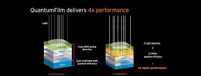
QuantumFilm Technology involves the creation of a film to coat the image sensors used in a cellphone camera, allowing it to capture more light, improving the quality of the images taken.[9][10] A typical camera phone pixel sensor is made up of several layers, with a layer of colored plastic or glass acting as a color filter sitting on top of several layers of metal connecting silicon electronic transistors together, which is itself on top of a base layer of silicon used by the sensor’s electronic transistors and photodetectors. The light coming to the sensor has to pass through the layers of metal before reaching the silicon, a weak light absorber, so the sensor detects only about 25 percent of the light that makes up the image.[11] QuantumFilm Technology places a layer of semiconducting crystals – called quantum dots – on top of the chip, which allows the chip to absorb more light, place more pixels in a smaller space, and create sharper images.[12]
Using quantum dots is more efficient at capturing light than traditional silicon-based image sensor chips (capturing 90-95% of the light that hits it), giving the sensors higher sensitivity in low light as well as higher resolution.[3][13] And while traditional image sensors read an image from top to bottom (which can create a blurred image when the subject is moving), quantum dots detect the entire image at the same moment, reducing the chance for distortion.[14]
Invisage holds patents related to the development of QuantumFilm technology, as well as its applications toward optoelectronic devices.[15]
found via Image Sensor World.