


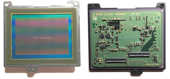

Landingfiled recently got an a7S III damaged from a laser light show. After removing the sensor cover glass they inspected the pixels under a 50x microscope objective:
It turns out this sensor has a 2×2 binning design. This means IMX510 actually has a 48MP native resolution. The RGGB Bayer pattern is spread across a 4×4 grid. After sensor readout, the four pixels in each pf the same color are then combined digitally to give one pixel before sending out on the SLVS-EC interface. This could explain the increase in read noise. From my knowledge, none of Sony DSLR CIS supports charge binning due to limitation in its pixel architecture. By combining four pixels digitally, you would increase the noise variance by four and hence read noise almost doubles (sqrt to RMS). The bright green pixels are phase detection pixel for hybrid AF system.
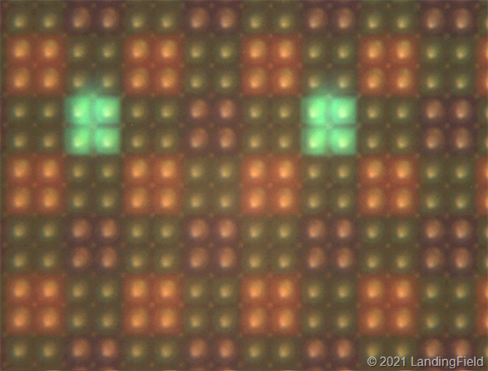

The 48MP Quad Bayer IMX510 sensor usees the 2×2 digital binning on it to produce a 12 megapixel bayer CFA output. Landingfield writes:
So the final question is why Sony went down this design path. I came up with two possible reasons. 1. Sony already has a BSI pixel design fitting this 4.2um pitch requirement. A 2×2 binning is a lot faster to reach market then starting off a new 8.4um pixel. Since most pixel design layouts are fixed, scaling the area can make multiple sizes of chip. For example, IMX411, IMX461, IMX455, IMX571 and IMX533 are all based on the same 3.76um BSI pixel design but each cover a different imaging circle from medium format to 1-inch. 2. Sony try to emphasis the HDR video capability on a7S III. A single pixel is limited in dynamic range. But you could read out each of the four sub-pixels with a different gain or exposure time. And later weight combining them digitally for the final value. Such method is used on many Sony security sensors. IMX294 and IMX482 also employ 2×2 binning BSI design.
Regardless of imaging quality, the third gen has a huge improvement in readout speed due to its BSI architecture. After all, this camera is mainly aimed for cinematographers. Its all-pixel scan rate has drastically increased from 30FPS to 90FPS. And 1080P60 no longer needs subsampling like in IMX235. Engineering has always been a balancing act. But still, it would be great to see a single large BSI pixel without microlenses achieving sCMOS grade quantum efficiency.
Thanks Landinfield for the great report (check out their website for more images).