Sony and Prophesee Develop a Stacked Event-Based Vision Sensor with the Industry’s Smallest Pixels and Highest HDR Performance

This isn’t sensor going to be usd on Sony Alpha camera. But it’s still interesting to see how advanced Sony’s tech is. In that case they managed to create a sensor with Industry’s Smallest Pixels and Highest HDR Performance
Press text:
Sony and Prophesee Develop a Stacked Event-Based Vision Sensor
with the Industry’s Smallest*1 Pixels and Highest*1 HDR Performance
- *1:Among stacked event-based vision sensors, as of announcement on February 19, 2020.
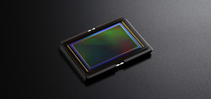
Tokyo, Japan—Sony Corporation and Prophesee S.A. today announced they have jointly developed a stacked event-based vision sensor with the industry’s smallest*1 4.86μm pixel size and the industry’s highest*1 124dB (or more) HDR performance. The new sensor and its performance results were announced at the International Solid-State Circuits Conference (ISSCC) held in San Francisco in the United States, starting on February 16, 2020.
The new stacked event-based vision sensor detects changes in the luminance of each pixel asynchronously and outputs data including coordinates and time only for the pixels where a change is detected, thereby enabling high efficiency, high speed, low latency data output. This vision sensor achieves high resolution, high speed, and high time resolution despite its small size and low power consumption. This accomplishment was made possible by combining technical features of Sony’s stacked CMOS image sensor, resulting in small pixel size and excellent low light performance that are achieved by the use of Cu-Cu connection*2, with Prophesee’s Metavision® event-based vision sensing technologies leading to fast pixel response, high temporal resolution and high throughput data readout. The newly developed sensor is suitable for various machine vision applications, such as detecting fast moving objects in a wide range of environments and conditions.
- *2:Technology that provides electrical continuity via connected Cu (copper) pads when stacking the back-illuminated CMOS image sensor section (top chip) and logic circuits (bottom chip). Compared with through-silicon via (TSV) wiring, where the connection is achieved by penetrating electrodes around the circumference of the pixel area, this method gives more freedom in design, improves productivity, allows for a more compact size, and increases performance. Sony announced this technology in December 2016 at the International Electron Devices Meeting (IEDM) in San Francisco.
Figure 1: Chip photographs

Pixel chip

Logic chip
Main Features
- Small size and high resolution delivered by stacked event-based vision sensor with the industry’s smallest*1 4.86μm pixel size
The pixel chip (top) and the logic chip (bottom) incorporate signal processing circuits which detect changes in luminance based on an asynchronous delta modulation method are arrayed separately. Each pixel of the two individual chips is electrically connected using Cu-Cu connection*2 in a stacked configuration. In addition to the industry’s smallest*1 4.86μm pixel size, the sensor also delivers 1/2 type, 1280×720 HD resolution by achieving high density integration with a fine 40nm logic process.
- Industry’s highest*1 124dB (or more) HDR performance achieved by high aperture ratio*3
The industry’s highest*1 124dB (or more) HDR performance is made possible by placing only back-illuminated pixels and a part of N-type MOS transistor on the pixel chip (top), thereby allowing the aperture ratio*3 to be enhanced by up to 77%. High sensitivity/low noise technologies Sony has developed over many years of CMOS image sensor development enable event detection in low-light conditions (40mlx).
- *3:Ratio of the aperture (other than the light-shielding portion) as viewed from the light incident surface side per pixel.
Figure 2: Pixel illustration

Conventional Sensor

Developed Sensor
3. Event data readout with high time resolution and high output
While a frame-based sensor outputs entire images at fixed intervals according to the frame rate, an event-based sensor selects pixel data asynchronously using a row selection arbiter circuit*4. By adding time information at 1μs precision to the pixel address where a change in luminance has occurred, event data readout with high time resolution is ensured. Furthermore, a high output event rate of 1.066Geps*5 has been achieved by efficiently compressing the event data, i.e. luminance change polarity, time, and x/y coordinate information for each event.
- *4:A circuit that determines the priority in the Y-axis direction corresponding to the requests from a plurality of pixels where a change in luminance has occurred.
- *5:The number of events per second.
Figure 3: Event data readout illustration

Trajectory of the ball

Frame-based sensor

Event-based sensor
Figure 4: Captured image example 1
- *Captured at night

Conventional sensor

Event-based sensor
Figure 5: Captured image example 2
- *Captured at night

Conventional Sensor

Event-based sensor
Key Specifications
| Process technology | 90nm BI CIS on 40nm CMOS | |
|---|---|---|
| Power supply voltage | 2.5, 1.1(V) | |
| Resolution | 1280×720 | |
| Pixel size | 4.86 x 4.86(µm2) | |
| Fill factor | >77% | |
| Power consumption | 100kEPS | 32(mW) |
| 300MEPS | 73(mW) | |
| Power/pixel | 35(nW) | |
| Energy/event | 137(pJ) | |
| Max event rate | 1066(MEPS) | |
| Timestamp resolution | 1(µs) | |
| Contrast sensitivity NCT | 15.7(% contrast) | |
| Low-light cutoff | 40(mlx) | |
| Dynamic range | >124dB | |