Sony A7R III Dissasembly and Teardown (by Ilija Melentijevic)

Ilija Melentijevic from Kolarivison disassembled the new Sony A7rIII. There are some interesting findings in his article that we are re-posting in full here:
Sony A7R III Dissasembly and Teardown
Our pre-ordered Sony A7R III finally arrived this morning, and we couldn’t wait to crack it open and see what’s inside. The A7R III has been receiving a lot of positive reviews and I can see why. First off, the camera looks and feels great. And, we finally got two card slots! The multi-selector and larger capacity battery are also a nice improvements. Beyond the cosmetics, the camera boasts significant improvements in frame rate, buffer capacity, light sensitivity, dynamic range, and more. I can go on, but I’ll leave that for the more detailed reviews. What we did notice is the camera is snappy. The A7 line has always had that signature shutter lag, it always felt like there was a slight delay from hitting that button to firing. With the A7R III, I am happy to say this is greatly improved; it feels like a more natural extension of the body. I think DSLRs might still be faster, but this is the first A7 series model that is competitive in that regard. We liked this camera so much, we almost decided not to tear it apart. Almost. We present you with the first look inside an A7R III.
One last look before we start.
We’ll start with the screws under the covers on the left side of the camera.
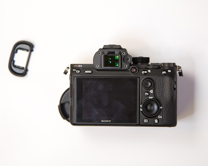
Next we take off the the eye cup and remove the 4 screws behind it as well as the diopter adjustment knob.
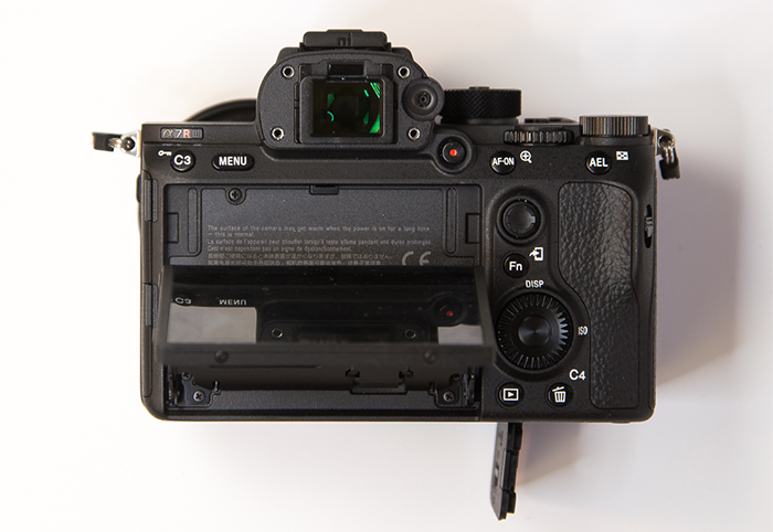
Several more screws behind the LCD hold the back plate on.
Under the card door there are 2 more screws that we remove.
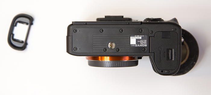
On the bottom of the camera, there are 8 screws holding down the name plate, and one more screw next to the battery door.
Removing the name plate reveals another plate. Another screw sits in the top of the battery compartment holding the top cover on.
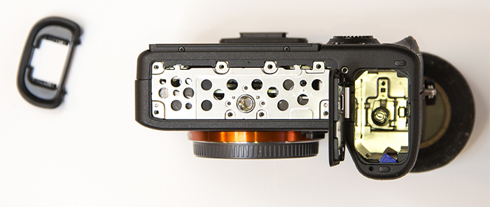
We remove the second plate showing the first glimpse of the interior. We can see the side of the image stabilization unit, and two conductive thermal pads attached to the frame here. Looks like Sony is distributing heat to the bottom rather than the back of the camera. At these capture rates this camera probably puts out a lot of heat.
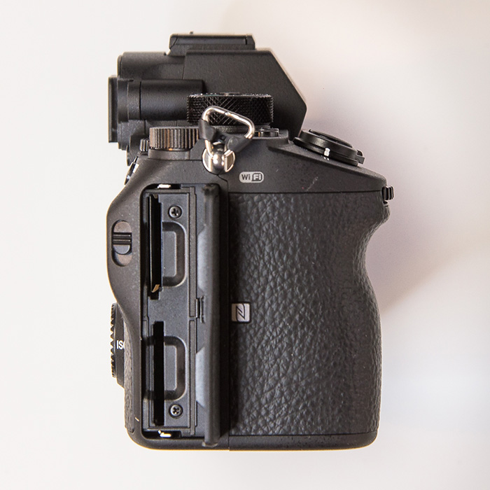
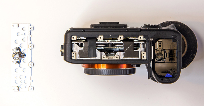
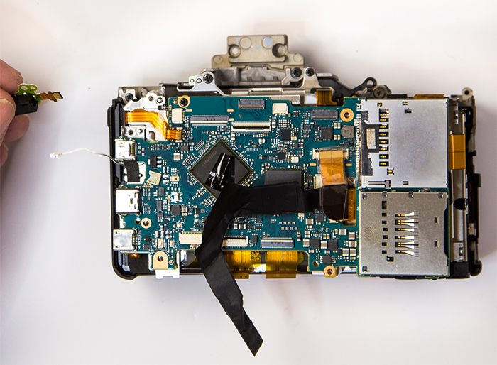
Taking the back off, the two card readers are very prominent. Only the top slot supports UHS-II cards, and it looks physically different than the bottom reader. We also immediately notice more conductive tape wrapping across the motherboard on top of the processors, and down to the frame. It even looks like the top reader has a thermal pad on it; Sony is taking heat dissipation very seriously, hopefully they have solved the heat issues they’ve had in the past.
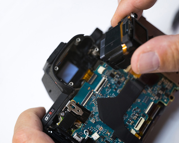
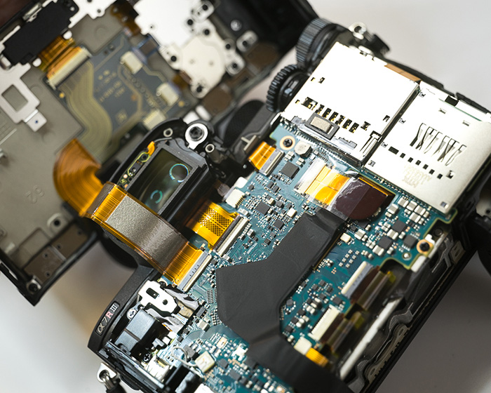
We disconnect the back panel and the viewfinder, and the viewfinder pulls away from the frame. It is held on with another thermal pad. Underneath the viewfinder cable there is another cable. Sony is very efficient with this board, putting cables under other cables in several places.
When we peal back the conductive tape, we get a first look at the processors. On the right, we see more flex cables under other cables , and even two that go through the board. We can almost take the motherboard off, but a bracket covers the last screw, so we have to remove the top cover. Two screws where the viewfinder was hold down the top cover.
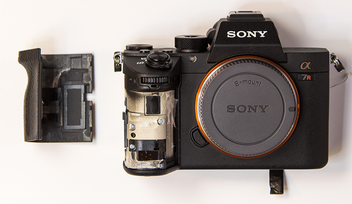
The top cover is still fixed, so we take off the front grip rubber to reveal several more screws.
With those screws out, we can remove the top cover, revealing that last screw.
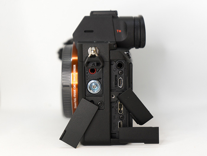
The 3.5mm microphone jack is a separate piece that we remove here.
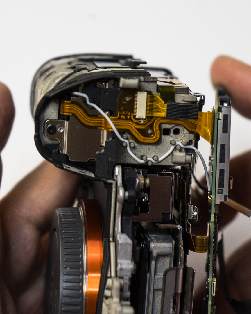
There are several cables underneath the motherboard which need to be removed before we can take out the motherboard. The antenna cable is routed very neatly.

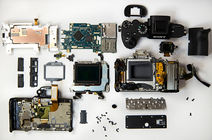
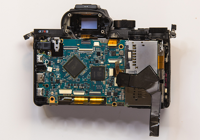
After disconnecting all of the motherboard cables (several were on the bottom side of the board and easy to miss), we can take a closer look at the motherboard.
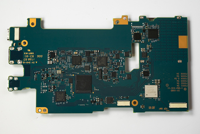
The underside of the motherboard. The three connectors are visible here, but otherwise this side is less busy.
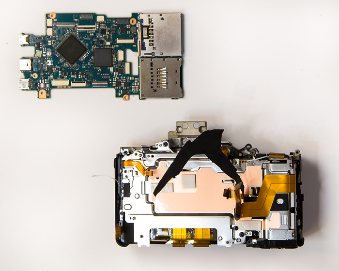
Underneath the motherboard there is a heavy shield and more thermal pads.
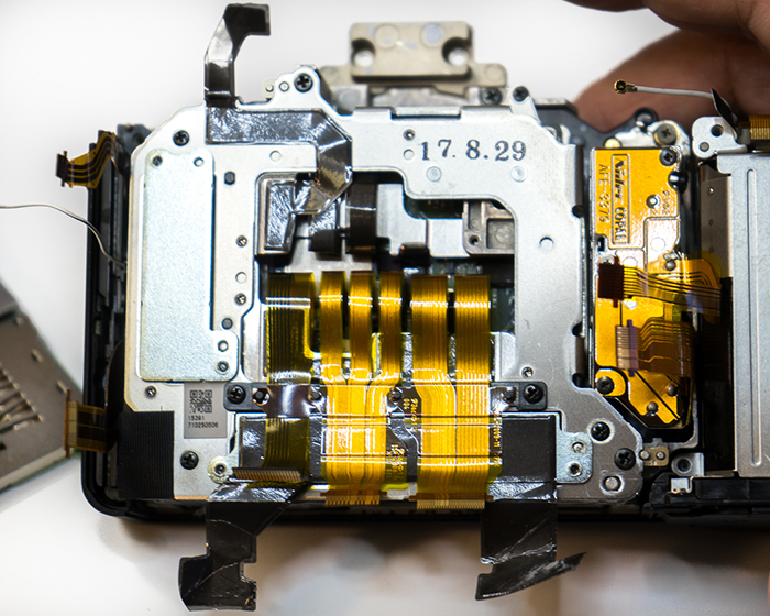
After removing the shield, we can see the image stabilization unit and yet more thermal tape. The sensor cables are split into several several thin sections. Presumably this makes the cables more flexible, which might help them handle the upgraded image stabilization system better.
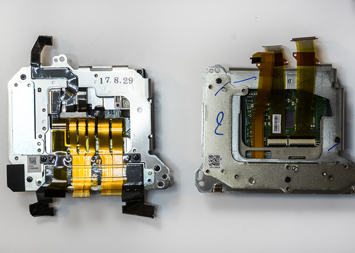
The A7R III image stabilizer on the left compared to the II generation. The new stabilizer is much beefier and is a clear upgrade. Notice how the II unit on the right doesn’t have any thermal tape.
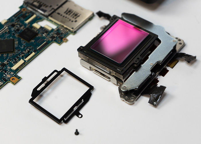
The image stabilizer and sensor come out as one unit, and we can now see the sensor. The sensor filter looks almost identical to the A7R II.
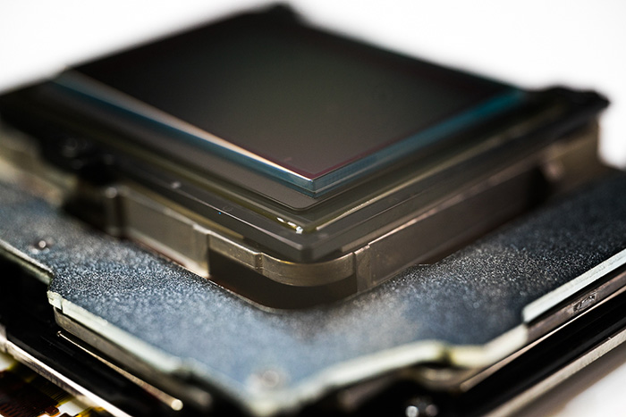
And yes, for anyone who was wondering, the sensor filter is still as thick as always. This means adapted lenses will still have degraded corners without our thin-filter modification.
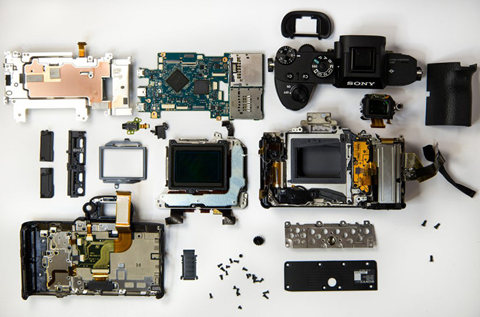
There you have it folks! The disassembled Sony A7R III. When we put it back together, it will have our thin filter installed.
–
Original article link: kolarivision.com/sony-a7r-iii-dissasembly-teardown/
Found via PetaPixel
–
Sony A7rIII at Amazon, Bhphoto, Adorama, BuyDig, FocusCamera, Calumet DE, Wex UK. Photo Porst Neuwied. Sony Netherland. Sony Australia. Sony Japan.
Sony 24-105mm at Amazon, Bhphoto, Adorama, BuyDig, FocusCamera, Amazon DE, Calumet DE, Wex UK.
Join the A7rIII facebook group to discuss the camera features and tests.